

last update: March 11, 2019
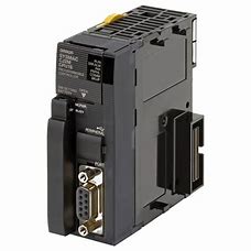
Analog Input Units CJ1W-AD041-V1/AD081-V1/AD042
| Item | CJ1W-AD041-V1 | CJ1W-AD081-V1 | CJ1W-AD042 | |||
|---|---|---|---|---|---|---|
| Unit type | CJ-series Special I/O Unit | |||||
| Isolation *1 | Between I/O and Controller signals: Photocoupler (No isolation between I/O signals.) |
Between I/O and Controller signals: Digital isolator (No isolation between I/O signals.) |
||||
| External terminals | 18-point detachable terminal block (M3 screws) | |||||
| Power consumption | 420 mA max. at 5 VDC | 520 mA max. at 5 VDC | ||||
| Dimensions (mm) | 31 × 90 × 65 mm (W × H × D) | |||||
| Weight | 140 g max. | 150 g max. | ||||
| General specifications | Conforms to general specifications for CJ Series. | |||||
| Input specifi- cations |
Number of analog inputs | 4 | 8 | 4 | ||
| Input signal range *2 | 1 to 5 V 0 to 5 V 0 to 10 V – 10 to 10 V 4 to 20 mA *3 |
1 to 5 V 0 to 10 V – 5 to 5 V – 10 to 10 V 4 to 20 mA *4 |
||||
| Maximum rated input (for 1 point) *5 |
Voltage Input: ± 15 V Current Input: ± 30 mA |
|||||
| Input impedance | Voltage Input: 1 MΩ min. Current Input: 250 Ω (rated value) | |||||
| Resolution | 4,000/8,000 *6 | 1 to 5 V | 10,000 | |||
| 0 to 10 V | 20,000 | |||||
| – 5 to 5 V | 20,000 | |||||
| – 10 to 10 V | 40,000 | |||||
| 4 to 20 mA | 10,000 | |||||
| Converted output data | 16-bit binary data | |||||
| Accuracy *7 |
25 °C *8 | Voltage Input: ± 0.2% of F.S. Current Input: ± 0.4% of F.S. | ||||
| 0 °C to 55 °C | Voltage Input: ± 0.4% of F.S. Current Input: ± 0.6% of F.S. | |||||
| A/D conversion period *9 | 1 ms/250 μs per point *6 | 20 μs/1 point, 25 μs/2 points, 30 μs/3 points, 35 μs/4 points |
||||
| Input functions |
Mean value processing | Stores the last “n” data conversions in the buffer, and stores the mean value of the conversion values. Buffer number: n = 2, 4, 8, 16, 32, 64 |
Stores the last “n” data conversions in the buffer, and stores the mean value of the conversion values. Buffer number: n = 2, 4, 8, 16, 32, 64, 128, 256, 512 |
|||
| Peak value holding | Stores the maximum conversion value while the Peak Value Hold Bit is ON. | |||||
| Scaling | — | Setting values in any specified unit within a range of ±32,000 as the upper and lower limits allows A/D conversion to be executed and analog signals to be output with these values as full scale. |
||||
| Input disconnection detection |
Detects the disconnection and turns ON the Disconnection Detection Flag. *10 | |||||
| Offset/gain adjustment | Supported | — | ||||
| Direct conversion | — | A/D conversion is performed and the converted value is refreshed when the ANALOG INPUT DIRECT CONVERSION instruction (AIDC) is executed. This instruction is supported by the CJ2H-CPU[][](-EIP) CPU Units with unit version 1.1 or later, and CJ2M-CPU[][]. CJ1, NJ501, and CP1H CPU Units and NSJ Controllers do not support direct conversion. |
||||
*1 Do not apply a voltage higher than 600 V to the terminal block when performing withstand voltage test on this Unit.
Otherwise, internal elements may deteriorate.
*2 Input signal ranges can be set for each input.
*3 Voltage input or current input are chosen by using the voltage/current switch at the back of the terminal block.
*4 To use a current input, connect the positive current input terminal and positive voltage input terminal with the enclosed
short bar.
*5 The Analog Input Unit must be operated according to the input specifications provided here. Operating the Unit outside
these specifications will cause the Unit to malfunction.
*6 The resolution can be set to 8,000 and the conversion period to 250 μs in the setting. There is only one setting for both
of these, i.e., they are both enabled or disabled together.
*7 The accuracy is given for full scale. For example, an accuracy of ±0.2% means a maximum error of ±8 (BCD) at a
resolution of 4,000.
For the CJ1W-AD041-V1/ AD081-V1, the default setting is adjusted for voltage input. To use current input, perform the
offset and gain adjustments as required.
*8 For the CJ1W-AD041-V1/ AD081-V1, 23±2°C.
*9 The A/D conversion period is the time required from when the Analog Input Unit receives the analog signal until it
stores the converted value in internal memory. It takes at least one cycle for the converted data to be stored in the
CPU Unit. (The direct conversion function of the CJ1W-AD042 is can be used to input data immediately to the CPU
Unit.)
*10 Line disconnection detection is supported only when the range is set to 1 to 5 V or 4 to 20 mA. If there is no input
signal when the 1 to 5 V or 4 to 20 mA range is set, the Line Disconnection Flag will turn ON.
Analog Output Units CJ1W-DA021/DA041/DA08V/DA08C/DA042V
| Item | CJ1W-DA021 | CJ1W-DA041 | CJ1W-DA08V | CJ1W-DA08C | CJ1W-DA042V | |||
|---|---|---|---|---|---|---|---|---|
| Unit type | CJ-series Special I/O Unit | |||||||
| Isolation *1 | Between I/O and Controller signals: Photocoupler (No isolation between I/O signals.) |
Between I/O and Controller signals: Digital isolator (No isolation between I/O signals.) |
||||||
| External terminals | 18-point detachable terminal block (M3 screws) | |||||||
| Power consumption | 5 VDC, 120 mA max. | 5 VDC, 140 mA max. | 5 VDC, 400 mA max. | |||||
| External power supply *2 | 24 VDC +10% -15%, (inrush current: 20 A max., pulse width: 1 ms min.) |
— | ||||||
| 140 mA max. | 200 mA max. | 140 mA max. | 170 mA max. | — | ||||
| Dimensions (mm) | 31 × 90 × 65 mm (W × H × D) | |||||||
| Weight | 150 g max. | |||||||
| General specifications | Conforms to general specifications for CJ-series Series. | |||||||
| Output specifi- cations |
Number of analog outputs | 2 | 4 | 8 | 8 | 4 | ||
| Output signal range *3 | 1 to 5 V/4 to 20 mA 0 to 5 V 0 to 10 V – 10 to 10 V |
1 to 5 V 0 to 5 V 0 to 10 V – 10 to 10 V |
4 to 20 mA | 1 to 5 V 0 to 10 V – 10 to 10 V |
||||
| Output impedance | 0.5 Ω max. (for voltage output) | 0.5 Ω max. (for voltage output) |
— | 0.5 Ω max. (for voltage output) |
||||
| Max. output current (for 1 point) |
12 mA (for voltage output) | 2.4 mA (for voltage output) |
— | 2 mA (for voltage output) |
||||
| Maximum permissible load resistance |
600 Ω (current output) | — | 350 Ω | — | ||||
| Resolution | 40,000 | 4,000/8,000 *8 | 1 to 5 V | 10,000 | ||||
| 0 to 10 V | 20,000 | |||||||
| -10 to 10 V | 40,000 | |||||||
| Set data | 16-bit binary data | |||||||
| Accuracy *4 |
25 °C | Voltage output: ± 0.3% of F.S. Current output: ± 0.5% of F.S. |
± 0.3% of F.S. | ± 0.3% of F.S. | ± 0.3% of F.S. | |||
| 0 °C to 55 °C | Voltage output: ± 0.5% of F.S. Current output: ± 0.8% of F.S. |
± 0.5% of F.S. | ± 0.6% of F.S. | ± 0.5% of F.S. | ||||
| D/A conversion period *5 | 1.0 ms per point | 1.0 ms or 250 μs per point *8 | 20 μs/1 point, 25 μs/2 points, 30 μs/3 points, 35 μs/4 points |
|||||
| Output functions |
Output hold function | Outputs the specified output status (CLR, HOLD, or MAX) under any of the following circumstances. When the Conversion Enable Bit is OFF. *6 In adjustment mode, when a value other than the output number is output during adjustment. *7 When output setting value error occurs or Controller operation stops. When the Load is OFF. |
||||||
| Scaling | — | Supported only for a conversion period of 1 ms and resolution of 4,000. Setting values in any specified unit within a range of ± 32,000 as the upper and lower limits allows D/A conversion to be executed and analog signals to be output with these values as full scale. |
Setting values in any specified unit within a range of ±32,000 as the upper and lower limits allows D/A conversion to be executed and analog signals to be output with these values as full scale. |
|||||
| Offset/gain adjustment | Supported | — | ||||||
| Direct conversion | — | D/A conversion is performed and the output value is refreshed when the ANALOG OUTPUT DIRECT CONVERSION instruction (AODC) is executed. This instruction is supported by the CJ2H- CPU[][](-EIP) CPU Units with unit version 1.1 or later, and CJ2M-CPU[][]. CJ1, NJ501, and CP1H CPU Units and NSJ Controllers do not support direct conversion. |
||||||